Jenoptik is responding to the growing demand for high-power laser diodes with technical modernization and higher levels of staffing.
Source: JENOPTIK AG
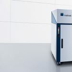
In Berlin, Jenoptik is investing in modern production equipment, so ensuring the long-term competitiveness in a photonic core business: Thanks to new machines and systems, Jenoptik can speed up order processing for the production of high-power laser diodes in the Adlershof Technology Park in Berlin, and is thus gearing up for a continuing high demand for semiconductor lasers. Jenoptik is one of the few independent specialists in the complete processing and technology chain, from laser semiconductor material to customer-specific application solutions.
A new, so-called stepper is used to manufacture laser diodes, and this increases production capacity, yield rate and quality. Delivery times are thus reduced. At the same time, there has been investment in new equipment for facet coating. In the medium term, investment in the low double-digit million euro range is planned in all three production areas of facet coating, wafer processing and epitaxy.
“Not only will we become faster, but we also guarantee the production and further development of state-of-the-art semiconductor lasers with very high power output“, says site manager Dr. Jürgen Sebastian.
The semiconductor bars manufactured by Jenoptik are increasingly used for example in the healthcare and life science sectors, for advanced manufacturing technologies as well as for cutting-edge sensor systems, which advance trends in the automotive industry such as autonomous driving.
Specialists for high-tech manufacturing
The expansion of production and clean rooms also leads to new employees: Jenoptik employs and hires specialists such as production engineers, microtechnologists, laboratory technicians and precision mechanics, as well as medical and chemical-technical assistants. Overall, at the Adlershof site the number of Jenoptik employees should increase to 75 by the end of the year. When the production facility opened in 2006, it had just 18 employees.
Jenoptik is also taking a new approach to training: With the Ferdinand Braun Institute, Leibniz Institute for High-Frequency Technology (FBH) located in Adlershof, Jenoptik has launched a training initiative supporting dual training at FBH. In concrete terms, this means that FBH trainees gain practical industrial experience at Jenoptik in the course of their training.
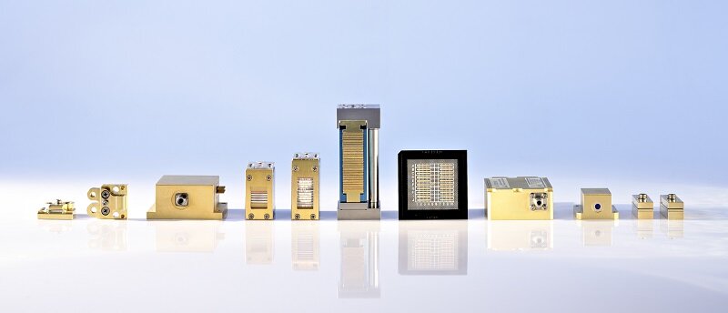
Semiconductor materials made by Jenoptik
In 2002, Jenoptik Diode Lab at the Berlin location was established as a spin-off from the Ferdinand Braun Institute, Leibniz Institute for High Frequency Technology (FBH). In 2006, Jenoptik opened the high-tech production of semiconductor lasers. The extension that followed in 2012 was one of the Jenoptik Group’s largest single investments, costing around 10 million euros. The 2,900 square meters, 950 square meters of which are clean rooms, is available for epitaxy, wafer processing and facet coating, providing the complete production line for manufacturing semiconductor lasers.
In the typical semiconductor manufacturing process, wafers are structured and processed into laser bars. The laser bars produced in Berlin are supplied to customers worldwide and are processed into high-power diode lasers, and at Jenoptik in Jena they are integrated into other laser systems.
Source:Jenoptik
More information:
On Jenoptik’s official website
RELATED NEWS
-
 Renishaw’s new pioneering encoder boldly goes into space
-
 Jenoptik presents fast and precise 3D laser metal cutting machine at Fabtech 2017
-
 TRUMPF presents the future of laser technology in Munich
-
 TRUMPF develops technology for high-brilliance direct diode lasers
-
 New flexible Hommel-Etamic AG380 snap gauge


